![[RS232 pinout diagram]](rs232.png)
| Contents | Index | Section 2 |
This manual provides a comprehensive description of the Amstrad PPC hardware and firmware. General information about the PPC and the delivered operating system software is contained in the Amstrad PPC User Instructions. This manual is intended to satisfy the needs of advanced developers who must have access to the various resources available within the PPC640 and PPC512.
Note that all address constants in this document are hexadecimal. In addition hexadecimal quantities are noted with small letter 'h' terminator to denote that they are in hexadecimal form. Address quantities are not usually annotated this way since they are clearly hexadecimal. Values are presented in hexadecimal form when they are logically bit oriented quantities rather than of purely numerical significance.
The CPU is a low power 8086-2 microprocessor with 1 Megabyte memory addressing capability (See Figure 1.1), running at a clock frequency of 8MHz. The CPU is connected to an on-board 16-bit system memory bus requiring four 125nS timing cycles (T-States) per access resulting in a 500nS memory cycle for 16-bit memory. The CPU is also connected on an on-board 8 bit I/O and memory peripheral bus with a 4 MHz clock, which in turn connects to an external expansion bus. Operations on the 8-bit bus automatically incur 125nS wait states as follows:
| Operation | Wait States | Bus Cycle |
|---|---|---|
| 8-bit (Memory) | 4 | 1.0 μS |
| 16 to 8-bit convert (Memory) | 12 | 2.0 μS |
| 8-bit (I/O) | 6 | 1.25 μS |
| 16 to 8-bit convert (I/O) | 16 | 2.5 μS |
The CPU is configured to run in maximum mode and the instruction set may be optionally extended by the addition of an 8087-2 Numeric Data Coprocessor. The 8087 BUSY output is connected directly to the 8086 NOT TEST input.
The main board memory consists of 640K bytes of system RAM with parity checking and 16K bytes of system ROM without parity checking.
The 640K byte user RAM starts at CPU memory address 00000 and extends to 9FFFF. Note that the PPC512 has 512K bytes installed memory ending at address 7FFFFh and the address space from 80000h to 9FFFFh may be extended in external 32K byte blocks (up to the 640K maximum).
The 128K byte address space from A0000 to BFFFF is reserved for video regeneration buffers, and is not used by CPU programs. The PPC Internal Display Adapter (IDA) uses the 64K byte address range from B0000 to BFFFF. The segmentation of this memory range is dependent on the display mode (See section 1.11). External display adapters also use this memory address range for their display buffers.
The 192K byte address space from C0000 to EFFFF is reserved for external expansion ROM address space. Hard Disk controllers use the range from C8000 to C9FFF. Additional hard disk controllers may also use the area from CA000 to CD000. The PPC test board uses the ROM area from E0000 to E7FFF.
The 16K byte system ROM is at FC000 to FFFFF and contains the Resident Operating System (ROS) firmware. The 48K byte address range from F0000 to FBFFF is reserved for ROM space expansion. The 16K byte ROS area address bits are partially decoded such that the ROS ROM repeats four times in the F0000 to FFFFF address range.
| 00000 | ON-BOARD DYNAMIC RAM |
640K
Byte System Memory |
||
| 9FFFF | ||||
| A0000 | 128K
BYTES VIDEO DISPLAY BUFFERS |
|||
| BFFFF | ||||
| 1M
BYTE ADDR RANGE |
C0000 | 192K
BYTES EXPANSION ROMS |
||
| EFFFF | ||||
| F0000 |
48K BYTES ROS ROM BLOCK REPEATS |
64K Byte System ROM area |
||
| FBFFF | ||||
| FC000 | 16K
BYTES (ROS) RESIDENT OPERATING SYSTEM ROM |
|||
| FFFFF | ||||
The interfaces on the main board occupy the 8086 I/O addresses as follows:
| ADDRESS(hex) | OUTPUT USE | INPUT USE |
|---|---|---|
| 000 - 00F | 8237 DMA Controller | 8237 DMA Controller |
| 010 - 01F | Do Not Use | Do Not Use |
| 020 - 021 | 8259 Interrupt control | 8259 Interrupt control |
| 022 - 03F | Do Not Use | Do Not Use |
| 040 - 042 | 8253 PIT Load Count (0-2) | 8253 PIT Read Count (0-2) |
| 043 | 8253 PIT Load Mode | Undefined |
| 044 - 05F | Do Not Use | Do Not Use |
| 060 | No Effect | Port A - Keyboard Code or System Status 1 |
| 061 | Port B - System Control | Port B - (Readback) |
| 062 | No Effect | Port C - System Status-2 |
| 063 | No Effect | Do Not Use |
| 064 | Write System Status-1 | Do Not Use |
| 065 | Write System Status-2 | Do Not Use |
| 066 | System Reset | Do Not Use |
| 067 - 06F | Do Not Use | Do Not Use |
| 070 | 146818 RTC Address | Do Not Use |
| 071 | 146818 RTC Data | 146818 RTC Data |
| 072 - 077 | Do Not Use | Do Not Use |
| 078 | Reserved | Reserved |
| 079 | Do Not Use | Do Not Use |
| 07A | Reserved | Reserved |
| 07B - 07F | Do Not Use | Do Not Use |
| 080 | Do Not Use | Do Not Use |
| 081 | DMA Page Register Ch 2 | Do Not Use |
| 082 | DMA Page Register Ch 3 | Do Not Use |
| 083 | DMA Page Register Ch 0,1 | Do Not Use |
| 084 - 09F | Do Not Use | Do Not Use |
| 0A0 | NMI Mask Control | Do Not Use |
| 0A1 - 0BF | Do Not Use | Do Not Use |
| 0C0 - 0FF | Reserved | Reserved |
| 2F8 - 2FF | Modem UART Tx Data/Control |
Modem UART Rx Data/Control |
| 378 | Printer Data Latch | Printer Data Latch |
| 379 | Do Not Use | Printer Status |
| 37A | Printer Control Latch | Printer Control Latch |
| 37B - 37F | Do Not Use | Do Not Use |
| 3B0 - 3B7 | Mono Mode CRTC Registers |
Mono Mode CRTC Registers |
| 3B8 - 3BF | Mono Mode Control Registers |
Mono Mode CRTC Registers |
| 3D0 - 3D7 | Colour Mode CRTC Registers |
Colour Mode CRTC Registers |
| 3D8 - 3DF | Colour Mode Control Registers |
Colour Mode Control Registers |
| 3F0 - 3F1 | Do Not Use | Do Not Use |
| 3F2 | Drive Selection | Do Not Use |
| 3F3 | Do Not Use | Do Not Use |
| 3F4 | Do Not Use | 765 FDC Status |
| 3F5 | 765 FDC Data | 765 FDC Data |
| 3F6 - 3F7 | Do Not Use | Do Not Use |
| 3F8 - 3FF | COM1 8250 UART Tx Data/Control |
COM1 8250 UART Rx Data/Control |
The 8086 CPU I/O addresses on the expansion bus are as follows:
| ADDRESS(hex) | USE |
|---|---|
| 200 - 20F | External Game Control Interface |
| 210 - 217 | External Bus Expansion Unit |
| 220 - 24F | Reserved |
| 278 - 27F | External Printer Port |
| 2F0 - 2FF | Reserved |
| 300 - 31F | External Prototyping Card |
| 320 - 32F | External Hard Disk Controller |
| 380 - 38F | External SDLC Serial RS232C Port |
| 3A0 - 3AF | Reserved |
| 3B0 - 3BB | External Monochrome VDU Controller |
| 3BC - 3BF | Printer Port |
| 3C0 - 3CF | External Graphics Controller |
| 3D0 - 3DF | External Colour/Graphics Controller |
I/O address above 03FFh, if accessed, wrap around and are mapped onto the range 0000h-03FFh.
External cluster controllers at 0790h-0793h, 0B90h-0B93h, 1390h-1393h and 2390h-2393h wrap around to I/O addresses 0390h-0393h respectively.
The Amstrad PPC supports four DMA channels on the system board, using an 8237-4 DMA controller and programmable page registers to extend its addressing range from 64k bytes to the full 1M byte processor address range. Each channel is able to transfer data in blocks of up to a maximum of 64K bytes within a page. The DMA channels are for 8-bit data transfers between (8-bit) I/O devices and 8-bit or 16-bit memory.
In peripheral (slave) mode, CPU I/O address lines A0 - A3 are connected conventionally so that 16 command codes appear in the order described in the 8237 data sheets (See section 3.5).
The DMA controller CLK is driven at 4MHz (+/- 0.1%). In master mode during DMA transfers on channels 1,2 and 3, one wait state is added resulting in a five-clock DMA bus cycle of 1.25μS. Channel 0 transfers have a four-clock bus cycle of 1μS.
The DMA channel request signals are as follows:
| DMA Channel | USE |
|---|---|
| 0 | 8253 Timer/Counter OUT1 output - for memory refresh. |
| 1 | Spare for use by expansion bus. Used by external SDLC Serial Port. |
| 2 | 765 Floppy Disk Controller DRQ output. Available on the expansion bus. |
| 3 | Spare for use by expansion bus. Used by external Hard Disk Controller. |
DMA channels 1, 2 and 3 can address the entire 1M byte addressing range of the CPU through the use of their associated DMA page registers. There are three DMA registers, one each for channels 1 through 3. Each page register defines for its channel which one of sixteen 64K byte pages in the 1M byte address range DMA transfers are to occur. The page registers are static so that modulo 64K byte addressing occurs at page boundaries.
The DMA page register bit assignments are as follows:
| Bit | Output Use |
|---|---|
| 7-4 | Not Connected |
| 3 | Address bit A19 |
| 2 | Address bit A18 |
| 1 | Address bit A17 |
| 0 | Address bit A16 |
Following a reset, system (ROS) initialisation firmware (in the ROS) sets up the 8237 DMA controller for channel 0 (dynamic refresh) operation as follows:
| Function | Initialised State |
|---|---|
| Word Count | 64K Transfers |
| Mode Register | Read Autoinitialise Increment Single Mode |
| Command Register | Disable Memory to Memory Enable Controller Normal Timing Fixed Priority Late Write DREQ Active High DACK Active Low |
| Mask Register | Clear Channel 0 Mask Bit |
After power-up or system reset the DMA page registers are undefined and are initialised to zero by the ROS firmware and all 8237 internal locations for channels 1-3 are initialised to a state comparable to the channel zero initialisation above.
Following industry compatibility, memory to memory DMA is not supported on the PPC. It is prohibited due to timing considerations.
Nine levels of hardware interrupt are provided for in the system by the CPU Non Maskable Interrupt (NMI) and by an 8259A-2 Interrupt Controller. All levels including NMI, are maskable under software control.
CPU I/O address line A0 is connected conventionally so that the command codes appear in the order described in the 8259 data sheets. The SP/EN pin is tied high signifying that the device is to be hardware un-buffered and designated as a master, not a slave.
The interrupt levels are assigned as follows:
| Level | Assigned Function |
|---|---|
| NMI | Memory Parity Error and 8087 NDP INT output. |
| 0 | 8253 Timer/Counter Out0 output. |
| 1 | Keyboard Scan Code Receiver. |
| 2 | 146818 Real Time Clock IRQ output. Available on the expansion bus. May be used by Enhanced Graphics Adapter |
| 3 | Used by Modem Serial Port (COM2) and external SDLC Serial Port. Available on the expansion bus. |
| 4 | Primary Serial port (COM1). Available on the expansion bus. Used by external SDLC Serial Port. |
| 5 | Hard Disk Controller. Available on the expansion bus. |
| 6 | 765 Floppy Disk Controller INT output. Available on the expansion bus. |
| 7 | Parallel Printer Port. Available on the expansion bus. Used by external Printer Port (secondary) and Printer Port (ternary) on external Monochrome VDU Controller. |
Following a reset, the initialisation firmware in the ROS sets the 8259 Interrupt Controller to operate as follows:
8086 system,
Single (not cascaded),
Normal fully nested (not special),
Edge-triggered,
Buffered mode - slave,
Normal EOI (not auto),
Fixed priority - level 0 highest, level 7 lowest.
The system (ROS) firmware initialises the 8259 address bits such that IRQ0 through IRQ7 appear in the CPU interrupt vector space at interrupts 8 through 15 respectrively. NMI is configured to CPU interrupt vector 2.
The NMI Mask Control is a write only register at I/O address 0A0h and allows the CPU non-maskable interrupt (NMI) input to be enabled or disabled by software. The Bit assignments are as follows:
| Bit | Output Use |
|---|---|
| 7 | Enable NMI. |
| 6 - 0 | Not Connected |
Following a reset NMI is disabled.
NMI can be connected to the 8087 NDP, the on-board memory parity check circuit, and the expansion bus I/OCHCK (I/O Channel Check).
Three programmable timer/counters are provided at I/O Addresses 040 - 043 by an 8253 Programmable Interval Timer (PIT) device. They are defined as follows:
| Counter | Use |
|---|---|
| 0 | General Purpose Timer. |
| 1 | Used by DMA channel 0 (for dynamic ram refresh). |
| 2 | Tone Generation for Speaker. |
The 8253 timers are configured as follows:
| Function | Configuration |
|---|---|
| CLK 0,1,2 | 1.193 MHz +/- 0.1% (54.925493 ms per count) |
| GATE 0,1 | Always 'ON'. |
| GATE 2 | Controlled via Port B (System Control Channel) Speaker Modulate output. |
| OUT 0 | Interrupts on 8259 PIC IR0 input. |
| OUT 1 | Requests on 8237 DMA DREQ0 input. |
| OUT 2 | Logical 'AND' with Port B (System Control Channel) Speaker Drive output. Also goes to Port C (System Status-2 Channel) as an input. |
Following a reset, the system initialisation firmware in the ROS programs the 8253 PIT for counter 1 (dynamic ram refresh) operation as a rate generator producing a signal with a period of 15.13 μS. There are no restrictions requiring the initialisation and programming of counters 0 and 2.
Two system status input channels and four output channels are provided on-board. Ports A, B and C emulate a pre-programmed 8255 PPI device. They are located in the I/O address space in the range 060h - 06Fh. Port B is programmed for control output, Port A is programmed either for Status-1 input or for receiving data from the keyboard, and Port C is programmed for Status-2 input.
Ports A, B and C emulate an 8255 PPI that has been set up as follows:
| Group A Mode 0, | Group B Mode 0, |
| Port A = input, | Port B = output, |
| Port C(U) = input. | Port C(L) = input. |
Unlike an 8255, power-up and reset do not affect this configuration.
The System Control channel is located at I/O Address 061h. Its bit assignment is as follows:
| Bit (PBn) | Output Use |
|---|---|
| 7 | Enable Status-1/Disable Keyboard Code on Port A. |
| 6 | Enable incoming Keyboard Clock. |
| 5 | Prevent external parity errors from causing NMI. (Also Disable any pending NMI). |
| 4 | Disable parity checking of on-board system Ram. |
| 3 | Undefined (Not Connected). |
| 2 | Enable Port C LSB / Disable MSB. (See 1.8.3) |
| 1 | Speaker Drive. |
| 0 | 8253 GATE 2 (Speaker Modulate). |
When bit 7 is set high, Status-1 data is enabled on Port A, the keyboard data path and keyboard interrupts are disabled. When bit 7 is set low, keyboard input data is enabled on port A, the keyboard data path and keyboard interrupts are enabled. Applications software which sets PB7 must restore it to the cleared state else the keyboard may be rendered inoperable.
The keyboard interface operates as follows: Each incoming keycode is latched on-board, causing a keyboard interrupt (on level 1). While the interrupt remains pending, the incoming keyboard data signal is forced low as an acknowledgement to the keyboard that the keycode has been received. As soon as the interrupt has been cleared, the keyboard may use the Data signal to transmit the next keycode.
PB5 when set prevents an external parity error (ie. an I/OCHCK condition on the expansion bus) from causing NMI, even if NMI is unmasked. When NMI has been triggered and latched it may be cleared by pulsing PB5 (if the external device has removed its I/OCHCK signal).
PB2 when set enables the reading of the four LS bits of the RAM fitted indicator on Port C. When PB2 is clear the top (MS) bit of the RAM fitted indicator is read (see 1.8.3).
PB1 may be toggled to drive the speaker with a corresponding pulse train. The speaker may also be driven by a wave form from the 8253 PIT OUT2 output (simultaneously with PB1).
PB0 may be toggled to drive the 8253 gate input, hence modulate counter 2 operations and therefore driving the speaker which may all be performed simultaneously to create various audio effects.
Port A is a read only location located at I/O Address 060h. The bit assignments for Port A are as follows:
| Bit (PAn) | Status-1 | Keyboard Input |
|---|---|---|
| 7 | Always 0. | KBD7 |
| 6 | Second Floppy disk drive installed. | KBD6 |
| 5 | DDM1 - Default Display Mode bit 1. | KBD5 |
| 4 | DDM0 - Default Display Mode bit 0. | KBD4 |
| 3 | Always 1. | KBD3 |
| 2 | Always 1. | KBD2 |
| 1 | 8087 NDP installed. | KBD1 |
| 0 | Always 1. | KBD0 |
When Port B, Bit 7 (PB7) is set to high, reading Port A loads Status-1. When PB7 is set low, reading Port A loads keyboard data.
The Default Display Mode bits (DDM1, DDM0) are set up by the ROS during system initialisation as follows:
| DDM1 | DDM0 | Default Display Mode Selected |
|---|---|---|
| 0 | 0 | External Extended Graphics Adapter Installed |
| 0 | 1 | Colour Graphics Adapter Emulation (or external CGA) with alpha, 40 X 25 chars, bright white on black. |
| 1 | 0 | Colour Graphics Adapter Emulation (or external CGA) with alpha, 80 X 25 chars, bright white on black. |
| 1 | 1 | Monochrome Display Adapter Emulation (or external MDA) with alpha, 80 X 25 chars. |
When the Internal Display Adapter (IDA) is enabled then switches 1 - 3 determine the IDA configuration and switches 4 & 5 determine the default display mode. See section 1.22 for these details.
Following a reset, the ROS then sets the initial video state is based on the DDM value. Section 2.3.7 gives additional details of the ROS Video Mode settings.
Port C is a read only location located at I/O Address 062h. Its bit assignments are as follows:
| Bit (PCn) | Input Use | |||||
|---|---|---|---|---|---|---|
| 7 | On-board system RAM parity error. | |||||
| 6 | External parity error (I/OCHCK from expansion bus). | |||||
| 5 | 8253 PIT OUT2 output. | |||||
| 4 | Undefined. | |||||
| LSB or MSB (depends on PB2) | ||||||
| 3 | RAM3 | Undefined | ||||
| 2 | RAM2 | Undefined | ||||
| 1 | RAM1 | Undefined | ||||
| 0 | RAM0 | RAM4 | ||||
PC7 is forced to the zero state when on-board system RAM parity checking is disabled by PB4.
When the I/OCHCK condition (external parity error) from the expansion bus is disabled from causing NMI (by PB5 set high), PC6 reflects the state of the I/OCHCK input else it reflects the latched state of I/OCHCK.
The value of RAM4-RAM0 denotes the amount of system RAM fitted to the system as follows:
| RAM4 | RAM3 | RAM2 | RAM1 | RAM0 | |
|---|---|---|---|---|---|
| 0 | 1 | 1 | 1 | 0 | 512K bytes. |
| 0 | 1 | 1 | 1 | 1 | 544K bytes. |
| 1 | 0 | 0 | 0 | 0 | 576K bytes. |
| 1 | 0 | 0 | 0 | 1 | 608K bytes. |
| 1 | 0 | 0 | 1 | 0 | 640K bytes. |
See section 1.8.1 for the Control Port B setting for reading RAM fitted segment bits.
The Write System Status-1 register (WSS1) is a write only register at I/O Address 064h and is initialised by the Resident Operating System (ROS) firmware based on values obtained from configuration switches 4 and 5. It is used in conjunction with the 8255 PPI Port A emulation. The bit assignments are as follows:
| Bit | Output Use |
|---|---|
| 7 | No effect. |
| 6 | PA6 - Second Floppy disk drive installed. |
| 5 | PA5 - DDM1. |
| 4 | PA4 - DDM0. |
| 3 | No effect. |
| 2 | No effect. |
| 1 | PA1 - 8087 NDP installed. |
| 0 | No effect. |
The Write System Status-2 register is a write only register at I/O Address 065h and is initialised by the Resident Operating System (ROS) firmware based on the memory size check perfomed during Power On Self Test. It is used in conjunction with the 8255 PPI Port C emulation. The bit assignments are as follows:
| Bit | Output Use |
|---|---|
| 7 | PC2 (MSB) - Undefined. |
| 6 | PC1 (MSB) - Undefined. |
| 5 | PC0 (MSB) - Undefined. |
| 4 | PC3 (MSB) - RAM4. |
| 3 | PC3 (LSB) - RAM3. |
| 2 | PC2 (LSB) - RAM2. |
| 1 | PC1 (LSB) - RAM1. |
| 0 | PC0 (LSB) - RAM0. |
Any write access to I/O Address 066h regardless of the value written will cause the hardware to generate an immediate 512μS system reset and pulse the reset line on the expansion bus. The contents of the on-board system RAM is preserved following a system reset.
A HD146818 Real Time Clock plus RAM device is installed and backed up by the battery pack. The clock device provides a time of day clock with alarm, a one hundred year calendar, a programmable periodic interrupt, and 50 bytes of static RAM. The static RAM is called the Non-Volatile RAM (NVR) and is used to store time of last usage. The ROS firmware maintains a checksum of the NVR and will reset the RTC to default configuration during startup whenever the checksum value is incorrect.
When system power is off and the 146818 is on battery backup power, the functions which remain active are the clock and the retention of RAM data.
The input crystal oscillator runs at 32.768 KHz and the 146818 interrupt request is connected to the 8259 system interrupt controller on level 2 (which is also available on the expansion bus). The 146818 power-sense input PS is connected to a battery condition sensor. When the backup battery voltage is sufficiently low, the VRT bit in register D becomes set indicating that the time, the calendar and the NVR data are no longer valid. When this condition is noted during startup, the firmware outputs the message "Please fit new batteries" and resets the NVR to default values (See section 2.5).
All the features described in the 146818 data sheet are available with the exceptions that the CKOUT (clock output) and SQW (square wave output) pins are not connected on the main board.
Writing or reading the NVR involves a two step sequence for each byte that is accessed. The RTC Address channel (I/O Address 070) is first loaded with the NVR location to be accessed. Then the RTC Data channel (I/O Address 071) is either written or read to complete the I/O operation. This facility should be used with caution in order to avoid disturbing the system configuration data.
The printer port provides an interface for driving 8-bit and 7-bit Centronics compatible printers. The timing of the signals to the printer is under direct software control. There is a read/write control latch for sending control signals to the printer, an unlatched read-only printer status channel, and a read/write data latch for sending printer data.
In addition the printer control latch can be read to obtain system type and switch information.
The printer data latch is a read/write record at I/O address 378 and its layout is as follows:
| Bit (Dn) | Output/Input Use | Cable Polarity |
|---|---|---|
| 7 | Data 7 | Hi |
| 6 | Data 6 | Hi |
| 5 | Data 5 | Hi |
| 4 | Data 4 | Hi |
| 3 | Data 3 | Hi |
| 2 | Data 2 | Hi |
| 1 | Data 1 | Hi |
| 0 | Data 0 | Hi |
The contents of the data latch are undefined following a power-up or system reset.
The printer control latch is a read/write record at I/O address 37A and its layout is as follows:
| Bit | Output/Input Use | Reset State | Cable Polarity |
|---|---|---|---|
| 7 | PPC SW 4 (inverted) [RO] | ||
| 6 | PPC SW 5 (inverted) [RO] | ||
| 5 | FDC Change Line [RO] | ||
| 4 | Enable Int on ACK | False | |
| 3 | Select Printer | False | Low |
| 2 | Not Reset Printer | True | Low |
| 1 | Select Auto Feed | False | Low |
| 0 | Data Strobe | False | Low |
Bit 7 is a read-only bit which reflects the state of switch 4 (at the side of the machine) and returns a logic "0" when the switch is in the "on" position and a logic "1" for the "off" position.
Bit 6 is a read-only bit which reflects the state of switch 5 and returns a logic "0" when the switch is in the "on" position and a logic "1" for the "off" position.
Bit 5 is diskette change line status and is true (logic "1") when the selected floppy disk's door is open or no diskette is installed. This signal is latched on the drive and remains true until the disk drive is selected and it receives a step pulse from the FDC. This bit is only valid when a floppy drive is active and selected.
When Interrupt on ACK is enabled an incoming Printer Acknowledge condition will cause a system interrupt on level 7 (which is also available on the expansion bus).
If the printer control lines normally driven via latched bits D0 - D3 are driven externally, the data read on input to this channel will be the logical OR of the latched bits and the externally driven bits, e.g. If a data bit is false and the corresponding cable bit is driven true by the external driver, the bit input will be true.
Following power-up or system reset, the control latch contents assume reset conditions as shown.
Note that this is a general purpose printer interface and that not all printers require all the control signals, hence the provision for non-standard printers to be able to drive some of the control signals as inputs to the main board. The timing requirements on Centronics compatible printers generally specify that data must be present at 1μS before the strobe is made active, and must remain valid for at least 1μS after strobe goes inactive. The strobe duration must be between 1μS and 500 μS. Printer Busy status can be inspected as soon as the strobe is inactive in order to determine when more data can be sent.
The Printer Status Channel is a read only register at I/O Address 0379h. Its layout is as follows:
| Bit | Input Use | Cable Polarity |
|---|---|---|
| 7 | -Printer Busy | High |
| 6 | -Printer Acknowledge | Low |
| 5 | Paper Out | High |
| 4 | Printer Selected | High |
| 3 | -Printer Error | Low |
| 2 | -LK3 fitted | |
| 1 | -LK2 fitted | |
| 0 | -LK1 fitted |
LK1 - LK3 are general purpose factory installed option links on the main board which are used by the system ROM Operating System (ROS) firmware to distinguish national variant machine configurations. The ROS will produce its sign-on message and error messages in one of seven languages. The first seven states (0 - 6) are used for language variants and the eighth (7) state is used extended diagnostic mode testing (See section section 2.2). Since the link state is inverted, the value obtained from the lower three bits of the printer port must be exclusive or'ed (XOR) with 1's to obtain the language number.
| LK1 | LK2 | LK3 | ROS Language |
|---|---|---|---|
| OFF | OFF | OFF | English. |
| OFF | OFF | ON | German. |
| OFF | ON | OFF | French. |
| OFF | ON | ON | Spanish. |
| ON | OFF | OFF | Danish. |
| ON | OFF | ON | Swedish. |
| ON | ON | OFF | Italian. |
| ON | ON | ON | Diagnostic Mode. (English) |
Note that this is a general purpose printer interface and that not all printers implement all the status lines, nor do they all attach the same meanings to the error conditions.
Printer Busy normally indicates that a printer cannot receive data, for example during data entry, printing, when offline, or during a printer error condition.
Printer Acknowledge, if implemented is generally asserted by a printer to indicate that data has been received and the printer is ready to receive the next data. Note that Printer Acknowledge (ACK) can also be set to cause interrupts (See 1.10.3).
Section 1.14 contains the printer connector pin assignments.
The Internal Display Adapter (IDA) is implemented using a gate array and a 6845 CRTC. It provides video for either the internal Liquid Crystal Display (LCD) or video output to a standard (PC1640) video connector at the rear of the PPC. The IDA is completely software compatible with the industry standard MDA & CGA environments and when outputting to an external display (in VDU mode) the video signals and scan frequencies are compatible with industry standard monitors.
The IDA provides either a Colour Graphics Adapter (CGA) emulation mode or a Monochrome Display Adapter (MDA) emulation mode. The video screen memory (or regeneration buffer) starting address is configured to B8000 for CGA emulation mode and to B0000 for MDA emulation mode.
The CGA display mode supports text or graphics in 16 colours on a Colour Display (CD) with a maximum resolution of 640 dots by 200 lines. Since colours cannot be displayed on the internal LCD a pixel will either be ON or OFF depending on whether it is the foreground colour or the background colour.
The MDA display mode supports black and white text in normal, intense, inverse, blink, or underline with a character cell resolution of 8 x 14. There are no graphics modes in MDA emulation mode. When using the internal LCD in MDA emulation mode the software environment is the same as that of a standard MDA device, but the character cell resolution is 8 x 8, intensified or highlighted characters are displayed with the vertical bars of each character one dot thinner than they would otherwise be and underlining is not supported.
In CGA emulation mode, the colour palette consists of sixteen colours as follows:
| Intensity | Red | Green | Blue | Colour |
|---|---|---|---|---|
| 0 | 0 | 0 | 0 | Black |
| 0 | 0 | 0 | 1 | Blue |
| 0 | 0 | 1 | 0 | Green |
| 0 | 0 | 1 | 1 | Cyan |
| 0 | 1 | 0 | 0 | Red |
| 0 | 1 | 0 | 1 | Magenta |
| 0 | 1 | 1 | 0 | Brown |
| 0 | 1 | 1 | 1 | White |
| 1 | 0 | 0 | 0 | Grey |
| 1 | 0 | 0 | 1 | Light Blue |
| 1 | 0 | 1 | 0 | Light Green |
| 1 | 0 | 1 | 1 | Light Cyan |
| 1 | 1 | 0 | 0 | Light Red |
| 1 | 1 | 0 | 1 | Light Magenta |
| 1 | 1 | 1 | 0 | Yellow |
| 1 | 1 | 1 | 1 | Intense White |
In colour mode, two Alpha modes are available: either 40 characters by 25 rows or 80 characters by 25 rows. The display RAM requirement is 2K bytes and 4K bytes of display RAM for 40 and 80 column modes respectively. The display regeneration buffer is from B8000h to BBFFFh for these modes and the ROS bios supports up to 8 or 4 separate display pages for 40 and 80 column modes respectively. This same display mapping is also repeated at BC000h.
The character set is formed by a ROM character generator and each of the 256 characters is made up of a 8 by 8 pixel matrix.
The starting address in the display RAM is programmed via the 6845 CRT (Cathode Ray Tube) Controller (CRTC). The starting address is on an even address boundary and it addresses the first (leftmost) character position in the top row of the display. The CRTC starting address register is a 16-bit register and it specifies the offset in two byte pairs from the display mode origin. This means for each change of one in the CRTC starting address register, the next even address is selected in the display RAM as the current regeneration buffer origin.
In order to display a single character, two bytes of display RAM are required, and for each pair of display RAM bytes, the even address is for the character code and the odd address is for the attribute byte. Subsequent characters are displayed along the row from left to right. When the end of a row is reached the next pair in the display RAM appears in the first character position of the next row down. Appendix 6 gives the 256 character codes and their respective default character representations.
The attribute byte allows a choice of either 16 foreground and 8 background colours per character, plus blinking, or a choice of 16 colours for both foreground and background without blinking.
The attribute byte for each is as follows:
| Bit (ATn) | Definition |
|---|---|
| 7 | Intensity or Enable Blink (Background) |
| 6 | Red (Background) |
| 5 | Green (Background) |
| 4 | Blue (Background) |
| 3 | Intensity (Foreground) or Character Map A/B Select |
| 2 | Red (Foreground) |
| 1 | Green (Foreground) |
| 0 | Blue (Foreground) |
Bit 7, the Intensity or Enable Blink Bit, changes function based the Mode Control Register. The Mode Control Register (I/O address 03D8h) bit 5 selects between Intensity or Blink.
When driving the internal LCD display in colour modes, the foreground and background colours are given the weightings such that Intensity = 1, Blue = 2, Red = 4, Green = 8 and compared. If the background has a higher value than the foreground the character is inverted. In addition, if bit 7 of the CGA mode control register (section 1.11.5) is set characters with non-black backgrounds are also inverted. These two inversion processes are cumulative so that characters may be doubly inverted and appear non-inverted. As with MDA characters on the LCD, text with an intensified foreground will have verticals one dot thinner.
CGA emulation mode supports graphics with 200 scan lines with a choice of two horizontal resolutions, either 320 pixels per scan line with four colours per pixel or 640 pixels per scan line with a two colours per pixel.
An additional low resolution mode is also supported with 100 scan lines and a horizontal resolution of 160 pixels per scan line with sixteen colours per pixel.
The regeneration buffer for colour graphics modes starts at B8000 and requires 16K bytes and is repeated at BC000. The ROS supports either 8 or 4 display buffer pages for the 320 or 640 resolution modes respectively.
Low resolution graphics mode is actually text mode and not a true bit mapped graphics mode in the sense that high and medium resolution graphics are. The CRTC is programmed such that there are 100 lines on the screen and the mode register is set up the same as text mode. There is no support for this mode in the ROS and the CRTC must be initialized as described in section 1.11.5.4.
In Low Resolution Graphics Mode (160x100), each logical pixel is mapped to a block of 4 x 2 physical pixels on the LCD. Each logical pixel also has 4 bits to determine which of the 16 colours it should be displayed in. These 4 bits are mapped directly to both rows of 4 physical pixels representing the logical pixels in question this providing 16 different pixel patterns to represent the 16 colours on the LCD.
The mapping of display ram in this graphics mode is actually an extension of the text mode scheme. The even bytes are all filled with a special graphics character, 0DEh, which contains a vertical bar. The odd bytes are then programmed in two four bit pairs with the leftmost pixel being the four high order bits. Each display line therefore requires 160 bytes and for the full 100 line display 16000 bytes are required.
The mapping of the odd byte(s) of graphics RAM in low resolution mode is as follows:
| RAM Bit: | 7 | 6 | 5 | 4 | 3 | 2 | 1 | 0 |
| Pixel: | 0 | 1 | ||||||
| Pixel Bit: | 3 | 2 | 1 | 0 | 3 | 2 | 1 | 0 |
In Medium Resolution Graphics Mode (320x200), the display memory for one scan line (320 pixels) consists of 80 bytes. Each pixel requires two bits so that four pixels are specified by each byte. The leftmost pixel is contained in the two MS bits of the byte and the two bit pairs for the remaining pixels follow on logically in left to right fashion. The two bit field for each pixel specifies one of four colours in one of three palettes as follows:
| Colour | Palette 0 | Palette 1 | Palette 2 |
|---|---|---|---|
| 0 | Background | Background | Background |
| 1 | Green | Cyan | Cyan |
| 2 | Red | Magenta | Red |
| 3 | Yellow | White | White |
In Medium Resolution LCD mode, each logical pixel is mapped to a pair of physical pixels on the LCD rather than a single pixel of a particular colour as described above. Changing palettes will not, therefore, change the display.
The display regeneration buffer for medium resolution graphics modes is mapped a split buffer configuration with the even scan lines (0, 2, 4, ... 198) contained in the graphics memory space from B8000 to B9F3F and the odd scan lines (1, 3, 5, ... 199) in the memory address range from BA000 to BBF3F. The memory map is as follows:
| 320 Pixels (2 Bits Per) | ||
|---|---|---|
| B8000 - | Scan Line 0 (80 Bytes) | - B804F |
| B8050 - | Scan Line 2 | - B809F |
| B80A0 - | Scan Line 4 | - B80EF |
| . | ||
| . | ||
| . | ||
| B9EF0 - | Scan Line 198 | - B9F3F |
| BA000 - | Scan Line 1 | - BA04F |
| BA050 - | Scan Line 3 | - BA09F |
| BA0A0 - | Scan Line 5 | - BA0EF |
| . | ||
| . | ||
| . | ||
| BBEF0 - | Scan Line 198 | - BBF3F |
The layout of a byte of graphics RAM in medium resolution mode is as follows:
| RAM Bit: | 7 | 6 | 5 | 4 | 3 | 2 | 1 | 0 |
|---|---|---|---|---|---|---|---|---|
| Pixel: | 0 | 1 | 2 | 3 | ||||
| Pixel Bit: | 1 | 0 | 1 | 0 | 1 | 0 | 1 | 0 |
In High Resolution Graphics Mode, the display memory for for one scan line consists of 80 bytes. Each pixel requires one bits so that eight pixels are specified by each byte. The leftmost pixel is contained in the MS bit of the byte and the remaining pixels follow from left to right. In high resolution mode the two colours are either black (pixel bit off) or pixel bit on with video in one of the 16 colours as selected by a foreground palette register.
One byte of graphics RAM in medium resolution graphics is as follows:
| RAM Bit: | 7 | 6 | 5 | 4 | 3 | 2 | 1 | 0 |
|---|---|---|---|---|---|---|---|---|
| Pixel: | 0 | 1 | 2 | 3 | 4 | 5 | 6 | 7 |
The address mapping of the scan lines in display RAM for high resolution graphics is the split buffer configuration depicted for medium resolution mode. - All (100) even scan lines from B8000 to B9F3F followed by all (100) odd scan lines from BA000 to BBF3F.
In monochrome mode there is only one Alpha mode available, 80 characters by 25 rows. When driving an external monochrome display, the character output is 8 x 14 pixel characters, whereas on the LCD a 8 x 8 character matrix is used.
The display RAM requirement is 4K bytes of display regeneration buffer area from B0000h to B0FFFh and is repeated in 1000h boundaries up to and including B7000h.
The 6845 CRTC Starting Address is programmed in the same way as in colour modes and the two byte character and attribute pairs are arranged in the display RAM just as in the colour modes. The attribute byte, however assumes different functions from the colour attributes since there are no IRGB signals sent to the monitor, but Video and Intensity are produced. The monochrome attribute byte is as follows:
| Function | Bits | 7 | 6 | 5 | 4 | 3 | 2 | 1 | 0 |
|---|---|---|---|---|---|---|---|---|---|
| Blanked | Bkg | I/B | 0 | 0 | 0 | I | 0 | 0 | 0 |
| Underlined | Bkg | I/B | 0 | 0 | 0 | I | 0 | 0 | 1 |
| Normal | Bkg | I/B | 0 | 0 | 0 | I | 1 | 1 | 1 |
| Inverse | Bkg | I/B | 1 | 1 | 1 | I | 0 | 0 | 0 |
Bit 7, the Background Intensity / Blink Enable (B/I) Bit, changes function based on the Mode control register. The Mode control Register (I/O address 03B8h) Bit 5 selects between Intensity or Blink Functions.
Bit 3 is the foreground intensity bit and controls the intensity when not in inverse video or blanked. The internal LCD displays higher intensity characters using a hardware algorithm to display the vertical lines one dot thinner than in normal intensity. Also, underlining is not supported on the LCD.
The ROS sets up the hardware to support eight different modes for the various displays available on the PPC range. The following table gives the modes supported by the ROS.
| ROS Mode | 0 | 1 | 2 | 3 | 4 | 5 | 6 | 7 |
|---|---|---|---|---|---|---|---|---|
| Type | Text | Text | Text | Text | Graph | Graph | Graph | Text |
| Columns | 40 | 40 | 80 | 80 | 320 | 320 | 640 | 80 |
| Rows | 25 | 25 | 25 | 25 | 200 | 200 | 200 | 25 |
| Colour(s) | 16 | 16 | 16 | 16 | 4 | B/W | 2 | Mono |
| Char Cell Size | 8x8 | 8x8 | 8x8 | 8x8 | 8x8 | 8x8 | 8x8 | 8x14 |
| Regen Origin | B8000 | B8000 | B8000 | B8000 | B8000 | B8000 | B8000 | B0000 |
| Regen Size | 16384 | 16384 | 16384 | 16384 | 16384 | 16384 | 16384 | 4096 |
| Page Size | 2048 | 2048 | 4096 | 4096 | 16384 | 16384 | 16384 | 4096 |
| Number Pages | 8 | 8 | 4 | 4 | 2 | 2 | 2 | 1 |
The Regeneration Buffer Origin is stated in hexadecimal notation since it is an address quantity. All other values are in decimal notation.
The ROS Video I/O supports multiple display pages and can be called to select an alternate page. The default (base page) upon initial mode selection is always zero and it begins at the origin address. The successive pages are located higher by the page size increment in the table. The equation for page origin is: Page Origin = Regen Origin + (Page Number - Page Size). Since the 'Page Size' quantity is a pure binary multiple it becomes a shift factor for the selected page number. Page are numbered from 0 to n-1 where 'n' is the number of pages available.
In colour mode there are seven registers for mode, colour selection, additional control functions.
The CGA Mode Control Register is a read/write register located at I/O address 3D8h. It is used to control the state of the video circuitry, selecting Alpha or Graphics mode and the various sub options available within Alpha and Graphics modes. On an industry standard CGA this is a write only register.
The layout of the CGA Mode control register is as follows:
| Bit | Output Use |
|---|---|
| 7 | LCD Inverse |
| 6 | LCD Lo-Res Graphics |
| 5 | Enable Blinking Chars (disable intensified backgrounds) |
| 4 | Select Graphics Mode 2 (de-select graphics mode 1) |
| 3 | Enable Video Display |
| 2 | Select Palette 2 (de-select palettes 0,1) |
| 1 | Select Graphics modes (de-select Alpha modes) |
| 0 | Select Alpha 80 Char mode (de-select 40 Char mode) |
Bit 0 is used for controlling 40 or 80 column text selection. When bit 0 is reset to "0" 40 column text is enabled. When bit 0 is set to "1" then 80 column text is enabled. Bit 0 has no effect Graphics modes.
Bit 1 selects between text and graphics modes. When bit 0 is reset to "0" then text mode is selected and when bit 0 is set to "1" then graphics mode is selected.
The Select Palette 2 bit (bit 2) has no effect in Alpha modes or in Graphics mode 2. It is used in conjunction with bit 5 of the VDU colour select register to control graphics mode 1 palette. To select palette 2, bit 5 of the CGA colour select register (below) should be reset and bit 2 of the VDU mode control register should then be set.
When bit 3 is reset to "0" the display is blanked by disabling foreground video. When bit 3 is set to "1" foreground video is enabled.
Bit 4 Selects between high resolution and medium resolution graphics modes. When bit 4 is set to "1" then 640x200 graphics resolution is selected and when bit 4 is reset to "0" then 320x200 graphics resolution is selected. Bit 4 has no effect in Alpha modes.
When bit 5 is set in Alpha modes, the foreground will blink for all displayed characters with attribute bit 7 also set. Bit 5 has no effect in Graphics modes.
Bit 6 provides hardware support for the CGA low resolution 160 x 100 sixteen colour graphics mode. It has no effect in external video mode but in LCD mode it enables each of the 16 colours to be displayed as a unique dot pattern.
Bit 7 adds an extra programmable feature to the interpretation of CGA text attributes when displayed on the LCD. When bit 7 is set to "1" in text mode, characters with non-black backgrounds will be displayed in inverse video. This inversion process is in addition to the non-programmable inversion which takes place place when the background colour is greater than the foreground. A character which is inverted by both of these processes will appear non-inverted. This inversion process effects the entire text screen on a character by character basis. This bit has no effect when driving an external CD display.
To avoid unsightly effects on the screen, this register should be updated during frame flyback time. Any kind of mode changing should preferably be done with video disabled. Mode changing involves the use of bits 1 and 0 and usually some re-programming of the CRTC.
The CGA Colour Select Register is a write only register located at I/O address 03D9h and is used for controlling border colour in alpha modes and for selecting palette, border and pixel colour options in the graphics modes. The layout of the CGA Colour select register is as follows:
| Bit | Alpha Modes | Graphics Mode 1 | Graphics Mode 2 |
|---|---|---|---|
| 7,6 | No Effect | No Effect | No effect |
| 5 | No Effect | Select Palette 1 (Deselect palette 0) | No effect |
| 4 | No Effect | Foreground Intensity for palettes 0, 1 & 2 | No effect |
| 3 | Intensity (Border) | Intensity (Backgnd and Border) | Intensity (Pixel) |
| 2 | Red (Border) | Red (Background and Border) | Red (Pixel) |
| 1 | Green (Border) | Green (Background and Border) | Green (Pixel) |
| 0 | Blue (Border) | Blue (Background and Border) | Blue (Pixel) |
In 640 x 200 two-colour graphics mode the overall screen palette is controlled by setting the CGA Colour Select register (which is initialized to 07h by the ROS on selection of mode 6). This means that the colour resolution is really one of 16 colours for foreground on a black background. Most applications software however control 640 x 200 mode graphics as black and white graphics.
To avoid unsightly effects on the screen this register should only be updated during frame flyback time.
The CGA Status Register is a read only register located at I/O address 03DA. It may be read at any time to determine the following:
| Bit | Input Use |
|---|---|
| 7 - 4 | Not used (always reset). |
| 3 | Frame Flyback (VSYNC) Time. |
| 2 | Light-pen switch made. |
| 1 | Light-pen latch set. |
| 0 | Display Enabled. |
Frame flyback time starts at the same time as the bottom border and lasts for 46 horizontal scan periods, ending 16 scans before the end of the subsequent top border.
Bit 2 reflects the state of the light-pen push button switch. Bit 2 = "1" when the light-pen switch is closed and bit 2 = "0" when the light-pen switch is open.
When bit 1 is set, it indicates that the light pen latch is set, triggered either by a pulse from the light pen or by writing data to set the light pen channel. Writing any data to the Clear Light Pen channel clears the latch.
Bit 0 = zero when the Video signal is enabled and bit 0 = "1" when either the vertical or horizontal retrace signals are active. This is a real time indication of the raster scan line status.
The 6845 CRTC is controlled by way of two I/O addresses, the CRTC Address register and the CRTC Data I/O location. The CRTC Address register is a write only register located at I/O address 3D4 and the lower 5 bits are used select the data register at I/O address 3D5. Addresses greater than 17 (11h) produce no results. Note that this set of I/O addresses is partially decoded such that all even I/O addresses between 3D0 - 3D6 access the CRTC index register and all odd I/O address between 3D1 - 3D7 access the selected CRTC data register.
The PPC gate array implementation incorporates a special "Auto-Switch" feature which enables the LCD to appear as a standard display device despite the fact that non-standard CRTC settings are required when dealing with the LCD. The auto-switch prevents CRTC registers 0 - 11 from being altered when bit 6 of the operation control port is set. Any attempt to write to these registers are trapped and PPC unique readback ports are provided so that the ROS's NMI service routine can readback the values written to these registers. Any write access to either the prohibited CRTC registers, the Operation Control port or the CGA control port will trigger a Non-Maskable Interrupt (NMI) when bit 7 of the Operation Control port is set. Bits 5-7 of the CRTC Index readback register can then be read by the NMI service routine to determine which of the three events triggered the NMI. In this way the NMI service routine is alerted to any attempted mode change and can change modes itself by loading the CRTC registers with the appropriate values for the operation in the desired LCD mode. The auto-switch also prevents accidental (non-ROS) changes to bits 6 and 7 of the CGA Control port.
The CRTC registers must be programmed according to the mode of operation required in conjunction with the CGA Mode and Colour Select Registers previously described. A mode changing operation should be performed in the following sequence: Disable video, reprogram the CRTC as required, reprogram the Mode and Colour select registers as required, (maintaining video disabled), initialize display RAM as required, enable video.
The CRTC registers are initialized for LCD CGA mode as follows:
| Register Number (Hex) |
Register Name | Alpha 40 Char Mode (Decimal) |
Alpha 80 Char Mode (Decimal) |
Graphics Low-res (Decimal) |
Graphics High-res (Decimal) |
|---|---|---|---|---|---|
| 00 | Horizontal Total (-1) | 41 | 83 | 83 | 43 |
| 01 | Horizontal Displayed | 40 | 80 | 80 | 40 |
| 02 | Horiz. Sync Position | 41 | 81 | 81 | 42 |
| 03 | Horiz. Sync Width | 01 | 01 | 01 | 01 |
| 04 | Vertical Total | 26 | 26 | 107 | 107 |
| 05 | Vertical Total Adjust | 0 | 0 | 0 | 0 |
| 06 | Vertical Displayed | 26 | 26 | 107 | 107 |
| 07 | Vertical Sync Position | 25 | 25 | 100 | 100 |
| 08 | Interlace | 2 | 2 | 2 | 2 |
| 09 | Max. Scan Address | 7 | 7 | 1 | 1 |
| 0A | Cursor Start | 6 | 6 | 6 | 6 |
| 0B | Cursor End | 7 | 7 | 7 | 7 |
| 0C | Start Address High | 0 | 0 | 0 | 0 |
| 0D | Start Address Low | 0 | 0 | 0 | 0 |
| 0E | Cursor Location High | 0 | 0 | 0 | 0 |
| 0F | Cursor Location Low | 0 | 0 | 0 | 0 |
Values greater than 31 in register 0Ah turn the cursor off. This is because bit 5 is the cursor off bit. Bit 6 in register 0Ah selects alternate blink rate.
Note that the values listed in the above two tables differ from the industry standard values used for other CGA devices. The user need not make special consideration when loading the CRTC but use the standard values as described in section 2.3.20. The auto switch NMI routine will adjust the CRTC values for the mode of operation as required.
A method of setting and clearing the light pen latch is provided as part of the IDA. Any read or write I/O access to port 03DBh clears the light pen latch and any read or write I/O to port 03DCh sets the light pen latch. The data read or written is ignored.
This register in a PPC unique register used to control and monitor the operational mode of the VDU/LCD gate array. It is an input/output port located at I/O address 3DEh.
The layout of the Operation Control/Status Register is as follows:
| Bit | Output Use | Input Use |
|---|---|---|
| 7 | Enable Auto-Switch NMI | NMI Enable Readback |
| 6 | CRTC Prohibit | CRTC Prohibit Readback |
| 5 | Not Used | PPC SW3 |
| 4 | Not Used | PPC SW2 |
| 3 | Not Used | PPC SW1 |
| 2 | Switch Out | Switch Out Readback |
| 1 | MDA/CGA Select | MDA/CGA Readback |
| 0 | VDU/LCD Select | VDU/LCD Readback |
Bit 0 (output) controls the selection of the video output. When bit 0 is set to "1" then video output is to the connector at the rear of the PPC. When Bit 0 is reset to "0" then the internal LCD is selected. Readback returns the information as written.
Bit 1 (output) controls the selection of the display type. When bit 1 is set to "1" then the PPC is setup as a monochrome device and video output, the display buffer, CRTC I/O addresses, and control registers are configured for monochrome. When bit 1 is reset to "0" then the PPC is configured as a colour device and the video output, display buffer, and I/O addresses are set for colour compatibility. Readback returns the information as written.
Bit 2 (output) controls whether the Internal Display Adapter is switched in or out. When bit 2 is set to "1" then the IDA video RAM cannot be read or written and IDA internal registers can be written but not read. The display will continue to be active. An external display adapter may be fitted and there will be no conflicts in either display RAM or display I/O addresses. When bit 2 is reset to "0" then the IDA is present and as configured by bits 0 and 1. In this case an external display adapter may be present but must not be in the same (colour/monochrome) mode else I/O address and regeneration buffer conflicts will occur. Readback returns the information as written.
Bit 3 is not used for output. Upon input Bit 3 returns the state of configuration switch 1 and returns "1" when the switch is ON and "0" when the switch is OFF.
Bit 4 is not used for output. Upon input Bit 4 returns the state of configuration switch 2 and returns "1" when the switch is ON and "0" when the switch is OFF.
Bit 5 is not used for output. Upon input Bit 5 returns the state of configuration switch 3 and returns "1" when the switch is ON and "0" when the switch is OFF.
Note that in practice the ROS uses configuration switches 1, 2 & 3 to set bits 0, 1 & 2 of the Operation Control Port so that the inputs on bits 3 through 5 are closely associated with the functions of bits 0 through 2.
Bit 6 (output) controls whether or not accesses to the CRTC will be prohibited and trapped by the auto switch NMI. Setting bit 6 to "1" allows writes to CRTC registers R0 - R11 to take place. Resetting bit 6 to "0" prohibits CPU access to the CRTC registers as part of the auto-switch mechanism. Readback returns the information as written.
Bit 7 (output) controls whether the auto-switch NMI is enabled or not. When bit 7 is set to "1" then a NMI will be generated when the CPU writes to a prohibited CRTC register. When bit 7 is "0" the NMI feature is turned off. Readback returns the information as written. Note that the NMI Mask Control register (section 1.6.3 at I/O address 0A0h) masks this and all other NMI inputs into the CPU.
The CRTC Index Readback is a read only register located at I/O address 3DDh. It is used by the auto-switch NMI process to determine which CRTC register was last addressed. In addition the MS bits contain additional information about the NMI process.
The layout of the CRTC Index Readback register is as follows:
| Bit | Input Use |
|---|---|
| 7 | CGA Control Port Written. |
| 6 | Operation Control Port Written |
| 5 | Prohibited CRTC register written. |
| 4 - 0 | CGA Control Port Written. |
Bits 0 - 4 contain the last value written to the CRTC Index register.
Bit 5 is "1" when NMI was caused by an attempted write to a prohibited CRTC register.
Bit 6 is "1" when NMI was caused by a write to the Operation Control port.
Bit 7 is "1" when NMI was caused by a write to the CGA Control port.
Bits 5 - 7 are reset by the trailing edge of a read of the CRTC Index Readback port and are set when a NMI is generated by the VDU/LCD gate array.
The CRTC Data Readback is a read only register located at I/O address 3DFh. It is used by the auto-switch NMI process to determine the value written to the last indexed CRTC register. Upon read of I/O address 3DFh the 8-bit returned value is the value as written.
When the PPC is in monochrome mode it supports the monochrome text software environment.
The MDA Mode Control Register is a write only register located at I/O address 3B8h. It is used to control the state of the video circuitry.
The format of the MDA Mode control register is as follows:
| Bit | Output Use |
|---|---|
| 7 | No effect |
| 6 | No effect |
| 5 | Enable Blinking Chars (disable intensified background) |
| 4 | No effect |
| 3 | Enable Video Display |
| 2 | No effect |
| 1 | No effect |
| 0 | Hi-res mode (no effect - always set) |
When bit 5 is set in the foreground will blink for all displayed characters with the blink (7) bit set in their attribute bytes.
Bit 3 must be set in order to enable the video output and when bit 3 is zero the display is blanked.
Bit 0 on the standard MDA is Hi-res mode but since this bit must be set to achieve anything sensible it is redundant and wired permanently set.
The MDA Status Register is a read only register located at I/O address 03BA. It may be read at any time to determine the following:
| Bit | Input Use |
|---|---|
| 7 - 4 | Not used (0). |
| 3 | Video. |
| 2 - 1 | Not used (0). |
| 0 | Horizontal Sync. |
Bit 0 = "0" when the Video signal is enabled. Bit 0 = "1" when the horizontal retrace is active.
Bit 3 = "1" when the mono video output pin (7) is active. This is a real time status of the raster scan line output.
The CRTC is controlled by way of two I/O addresses, the CRTC Address register and the CRTC Data I/O location. The CRTC Address register is a write only register located at I/O address 3B0 and the lower 5 bits are used select the data register at I/O address 3B1. Addresses greater than 17 (11h) produce no results. Note that this set of I/O addresses is partially decoded such that all even I/O addreses between 3B0 - 3B6 access the CRTC index register and all odd I/O addresses between 3B1 - 3B7 access the selected CRTC data register.
The CRTC registers names and initial values are as follows:
| Register Number (Hex) |
Register Name | Text 80- Col VDU (Decimal) |
Text 80- Col LCD (Decimal) |
|---|---|---|---|
| 00 | Horizontal Total (-1) | 97 | 83 |
| 01 | Horizontal Displayed | 80 | 80 |
| 02 | Horiz. Sync Position | 83 | 81 |
| 03 | Horiz. Sync Width | 15 | 1 |
| 04 | Vertical Total (-1) | 25 | 26 |
| 05 | Vertical Total Adjust | 6 | 0 |
| 06 | Vertical Displayed | 25 | 26 |
| 07 | Vertical Sync Position | 25 | 25 |
| 08 | Interlace | 2 | 2 |
| 09 | Maximum Scan | 13 | 7 |
| 0A | Cursor Start | 11 | 6 |
| 0B | Cursor End | 12 | 7 |
| 0C | Start Address High | 0 | 0 |
| 0D | Start Address Low | 0 | 0 |
Setting bit 5 in register 0Ah turns the cursor off. Bit 6 in 0Ah selects alternate blink rate.
Note that the values listed in the above table differ from the industry standard for other monochrome devices. The user need not make special consideration when loading the CRTC but use the standard values as described in section 2.3.20. The auto switch NMI will adjust the CRTC values for the mode of operation as required.
The floppy disk controller is based on the NEC uPD765A single chip controller, and supports one or two 5.25 inch single or double sided, MFM double density floppy disk drives with a data rate of 250 kilobits per second.
The FDC is controlled by way of the Drive Selection register at I/O Address 03F2h. It is defined as follows:
| Bit (Dn) | Output Use |
|---|---|
| 7 - 6 | No effect |
| 5 | Switch motor(s) on and enable drive 1 selection |
| 4 | Switch motor(s) on and enable drive 0 selection |
| 3 | Allow 765A FDC to interrupt and request DMA |
| 2 | - 765A reset |
| 1 | Drive Select Bit 1 (DS1) |
| 0 | Drive Select Bit 0 (DS0) |
The Drive Select bits (DS1, DS0) are only valid for values of 00 and 01 for drives 0 and 1 respectively. The drive selection qualification is only completed when either bit 4 (for drive 0) or bit 5 (for drive 1) is set. In addition setting bits 4 or 5 will have no effect until the value of DS1, DS0 is correspondingly set.
Bit 2 (- 765A reset) must brought low (output as '0') and held low for at least 3.5 μs in order to reset the 765A. It must then be set high in order to release the reset signal.
On power-up or following a system reset, all bits in this register are cleared to zero.
The hardware imposes the following conditions on the use of the 765A controller and disk drives:
The asynchronous serial port is configured to I/O addresses 3F8h - 3FFh and is based on the National INS8250 ACE (or UART), single channel device.
The clock frequency input of the 8250 is 1.8432 MHz (± 0.1%).
The 8250 BAUD OUT output is connected to the RCLK input.
An interrupt level is available for use by the 8250. When the 8250 OUT2 output is driven low (i.e. a '1' is written to bit 2 of the 8250 MODEM Control Register) then the INTRPT signal is connected to the interrupt control IRQ4 input.
The serial interface uses a 25-way subminiature D type plug (male) connector emulating a DTE (Data Terminal Equipment).
The electrical levels of signal lines on this interface conform with EIA (Electronics Industry Association) standard RS-232C (and the equivalent V.24 interface standard).
The RS232C drivers and receivers between the 8250 and the serial channel connector are all inverting.
| Pin | EIA | CCITT | Description |
|---|---|---|---|
| 2 | BA | 103 | TxD - Serial Data Output |
| 3 | BB | 104 | RxD - Serial Data Input |
| *4 | CA | 105 | RTS - Request to Send Output |
| 5 | CB | 106 | CTS - Clear to Send Output |
| 6 | CC | 107 | DSR - Data Set Ready Input |
| 7 | AB | 102 | Signal Ground (Common Return) |
| 8 | CF | 109 | DCD - Data Carrier Detect Input |
| *20 | CD | 108.2 | DTR - Data Terminal Ready Output |
| 22 | DE | 125 | RI - Ring Indicator Input |
* These interchange circuits, where implemented, shall be used to detect either a power off condition in the equipment across the interface, or the disconnection of the interconnecting cable. The terminator for these circuits shall interpret the power off condition or the disconnection of the interconnecting cable as an OFF condition.
See Appendix 3 for additional details of serial signals and cable connections.
The parallel printer port is described in Section 1.10 and is a general purpose 'Centronics' style 8-bit interface. The printer interface uses a 25-way subminiature 'D' socket (female) connector located at the back of the PPC.
The Pin assignments for the printer connector is as follows:
| Pin | Assignment |
|---|---|
| 1 | Not Data Strobe |
| 2 | Data Bit 0 |
| 3 | Data Bit 1 |
| 4 | Data Bit 2 |
| 5 | Data Bit 3 |
| 6 | Data Bit 4 |
| 7 | Data Bit 5 |
| 8 | Data Bit 6 |
| 9 | Data Bit 7 |
| 10 | Not Printer Acknowledge |
| 11 | Printer Busy |
| 12 | Paper Out |
| 13 | Select Printer |
| 14 | Not Select Auto Feed |
| 15 | Not Printer Error |
| 16 | Not Reset Printer |
| 17 | Not Printer Selected |
| 18 | GND |
| 19 | GND |
| 20 | GND |
| 21 | GND |
| 22 | GND |
| 23 | GND |
| 24 | GND |
| 25 | GND |
![[Parallel pinout]](parallel.png)
Appendix 4 contains the Amstrad PL-2 printer lead specification.
Keyboard data input to the CPU is via the 8255 PPI Port A, and the keyboard interrupt (level 1) of the 8259A PIC. Both of these have been previously described in sections 1.6 and 1.8.
The Serial Clock and Serial Data signals are used for keyboard interface. These two bidirectional signals are used by the keyboard microcontroller to send keycodes to the main electronics board. The main electronics board also uses the same two signals to indicate readiness to receive another keycode back to the microcontroller. In addition these two signals are used to reset the microcontroller under hardware or software control.
The quiescent state for both Serial Clock and Serial Data is high. A minimum of 5 μs must separate a transition of one signal from another transition of the same signal, or any transition of the other signal.
Keycodes are sent from the keyboard microcontroller to the main board in 8-bit serial form MS bit first. Keycode data received by the main board is clocked into a shift register as either a "1" bit sequence or as a "0" bit sequence. To be interpreted as a "1" bit, the Serial Data signal must remain high during the time period when Serial Clock goes low and returns to the high state. To be interpreted as a "0" bit, Serial Data must be low prior to the Serial Clock transition from high to low, Serial Data will then go high followed by Serial Clock. The "1" bit or the "0" bit is clocked into the shift register on the falling edge of Serial Clock.
Upon receiving a keystroke from the microcontroller, within 5 μs of the last clock falling edge, the main board electronics drives the Serial Data line low and maintains it low until it is ready to receive a new keystroke. When the main board returns the Serial Data signal to the high state the microcontroller is free to send another keystroke. This response to the reception of a keycode is termed the ACKNOWLEDGE sequence.
The mainboard electronics causes a RESET to the keyboard microcontroller by driving the Serial Clock line low for 10 milliseconds or more. The state of the Serial Data signal does not affect the reset sequence.
The 8-bit keyboard data is capable of 128 'make' codes correspondingly 128 'break' codes. For any key which is pressed, the 'make' keycode produced is in the range of 0 - 127 decimal. When a key is released, the 'break' keycode produced is the same as the make keycode except that the top bit is set so that the value is in the range of 128 - 511 (decimal). A number of keys (such as the dedicated keypad keys) send an extended keycode sequence which identify them uniquely as dedicated keys rather than the numeric keypad set. The typical extended keycode sequence consists of an extended keycode identifier, 224 (E0h), followed by the keycode.
After a key is pressed and the keycode has been sent to the main board electronics, if no new keys are pressed and the key has remained pressed for more that one half second, then the keyboard microcontroller re-sends the keycode every 83 milliseconds provided that the main board indicates by an Acknowledge sequence that is ready to accept a new keycode. The Pause/Break key does not repeat.
The keycode 0AAh is sent after a reset to indicate successful completion of power-up tests.
The PPC ROM BIOS receives the keycodes via an interrupt subroutine and it 'tokenizes' them into a two-bytes value for further conversion to ascii values by applications software which use the tokenized keyboard information. The keycodes and their corresponding token values are covered in the ROS firmware (Section 2.3.4).
The modem serial port is configured to I/O addresses 2F8h - 2FFh (COM2). It is based on the National INS8250 ACE (or UART), single channel device.
The clock frequency of the 8250 is 1.8432 MHz (+/- 0.1%).
The 8250 BAUD OUT output is connected to the RCLK input.
An interrupt level is available for use by the 8250. When the 8250 OUT2 output is driven low (i.e. a '1' is written to bit 2 of the 8250 MODEM Control Register) then the INTRPT signal is connected to the interrupt control IRQ3 input.
The Modem (Hayes) AT commadn interface and register set details are documented in the Amstrad PPC User Instructions.
The modem connector is a BT type 431A connector located in a small covered compartment to the right of the LCD. A telephone extension socket consisting of a BT type 603A socket is provided at the right hand rear of the case. When the modem is not in use the connection is straight through so that the telephone can be used in standard voice mode.
The modem connector pin assignments are as follows:
| Pin | Assignment |
|---|---|
| 1 | Not Connected. |
| 2 | Line A |
| 3 | Local Earth. |
| 4 | Dialing Shunt. |
| 5 | Line B. |
| 6 | Not Connected. |
Note that pins 3 and 4 are not connected to the modem.
The USA version modem does not use the extension lead arrangement as with the UK modem. Instead the USA modem has two BELL telephone connectors at the rear of the mdoem labelled LINE and PHONE. It is intended that the user supply a telephone extension lead and that the extension lead be connected between the wall connector and the modem LINE connector and the telephone which was connected to the wall socket be connected to the modem PHONE connection. The US telephone wiring uses a two wire circuit and the inner two pins of the BELL connector are the line A & B connections.
The AMSTRAD PPC Supports a standard light pen interface via the 6845 CRTC. The Light Pen connector is located inside the PPC case on the left hand edge of the lower main board about 3 inches forward of the configuration DIP switches. It consisists of a 6-way berg strip and is labeled LIGHT PEN in large letters. Pin 1 is the forward most pin viewed from in front of the machine.
The pin assignment is as follows:
| Pin | Assignment |
|---|---|
| 1 | -Light Pen Input. |
| 2 | (Keyway) |
| 3 | -Light Pen Switch. |
| 4 | Ground. |
| 5 | +5 Volts DC. |
| 6 | +12 Volts DC. |
At the rear of the PPC there are two large 'D' socket connectors labelled 'Expansion A-B' and these allow the connection of external devices to the expansion bus.
Expansion Connector A is a 25-way D-socket containing the following signals:
| Pin | Signal | In/Out |
|---|---|---|
| 1 | +5 Volts DC | In |
| 2 | T/C | Out |
| 3 | I/O & Memory Address Bit A19 | Out |
| 4 | I/O & Memory Address Bit A17 | Out |
| 5 | I/O & Memory Address Bit A15 | Out |
| 6 | I/O & Memory Address Bit A13 | Out |
| 7 | I/O & Memory Address Bit A11 | Out |
| 8 | I/O & Memory Address Bit A09 | Out |
| 9* | I/O & Memory Address Bit A07 | Out |
| 10* | I/O & Memory Address Bit A05 | Out |
| 11* | I/O & Memory Address Bit A03 | Out |
| 12* | I/O & Memory Address Bit A01 | Out |
| 13 | AEN - Address Enable | Out |
| 14 | Ground | In |
| 15 | -DACK0 | Out |
| 16 | I/O & Memory Address Bit A18 | Out |
| 17 | I/O & Memory Address Bit A16 | Out |
| 18 | I/O & Memory Address Bit A14 | Out |
| 19 | I/O & Memory Address Bit A12 | Out |
| 20 | I/O & Memory Address Bit A10 | Out |
| 21 | I/O & Memory Address Bit A08 | Out |
| 22* | I/O & Memory Address Bit A06 | Out |
| 23* | I/O & Memory Address Bit A04 | Out |
| 24* | I/O & Memory Address Bit A02 | Out |
| 25* | I/O & Memory Address Bit A00 | Out |
Expansion Connector B is a 37-way D-socket containing the following signals:
| Pin | Signal | In/Out |
|---|---|---|
| 1 | -20 Volts DC | -- |
| 2 | IRQ2 | In |
| 3 | IRQ4 | In |
| 4 | IRQ6 | In |
| 5 | I/O RDY | In |
| 6 | -DACK2 | Out |
| 7 | -I/O CHCK | In |
| 8 | DREQ2 | In |
| 9* | CK14 (OSC) | Out |
| 10* | -MEMR (Memory Read) | Out |
| 11* | -IOR (I/O Read) | In/Out |
| 12* | ALE | Out |
| 13** | I/O & Memory Data Bit D7 | In/Out |
| 14** | I/O & Memory Data Bit D5 | In/Out |
| 15** | I/O & Memory Data Bit D3 | In/Out |
| 16** | I/O & Memory Data Bit D1 | In/Out |
| 17 | - 5 Volts DC | In |
| 18 | - 12 Volts DC | In |
| 19 | Ground | In |
| 20 | External Power (+12V) | In |
| 21 | IRQ3 | In |
| 22 | IRQ5 | In |
| 23 | IRQ7 | In |
| 24 | -DACK1 | Out |
| 25 | -DACK3 | Out |
| 26 | DREQ1 | In |
| 27 | DREQ3 | In |
| 28* | -MEMW (Memory Write) | Out |
| 29* | -IOW (I/O Write) | In/Out |
| 30* | RESET | Out |
| 31* | CK4 (CLOCK) | Out |
| 32** | I/O & Memory Data Bit D6 | In/Out |
| 33** | I/O & Memory Data Bit D4 | In/Out |
| 34** | I/O & Memory Data Bit D2 | In/Out |
| 35** | I/O & Memory Data Bit D0 | In/Out |
| 36 | + 12 Volts DC | In |
| 37 | + 5 Volts DC | In |
![[Expansion bus pinout]](expansion.png)
Expansion A-B
Erratum: The illustration shows sockets with too many pins. See annotated image. (Thanks to Jeb Mayers)
Note that the power pins (+5v-20V, -5V-12V, +12V) are listed as inputs, this means the power is to be supplied to, rather than drawn from, these parts.
The signals marked with an asterisk (*) after the pin number are generated directly from the internal gate arrays and should be buffered using a suitable non-inverting buffer (74HC244). There are a total of 16 such signals.
The signals marked with two asterisks (**) after the pin number are the expansion data bus and are at cmos levels. They should be pulled up to TTL levels with 10K ohm resistors.
All remaining signals are TTL compatible and can support a maximum loading of six low-power schottky (LSTTL) loads.
When an expansion unit is fitted, the PPC must be powered via the expansion connectors. PPC power requirements are:
+12V ±5% 50mA
+5V ±5% 2.5A
-5V ±5% 50mA
-12V ±5% 50mA
-20V ±5% 30mA
In addition, the input signal External Power (pin B20) must be connected to +12 Volts to disable the interal switching regulator. Other sources of power (monitor, battery, AC adapter) should be disconnected.
Note that direct access to the on-board 16-bit fast memory bus is not available via the I/O expansion connectors.
Additional engineering details of PPC circuitry can be obtained from the Amstrad PPC Service Manual which is availale as advised by Amstrad Customer Services.
Note: The USA version of the PPC has the expansion connectors covered by a piece of metal to satisfy FCC requirements.
The video connector a 9-way D type (female) socket located in the rear of the computer. Its pinout is as follows:
| Pin | Assignment | |
|---|---|---|
| 1 | Ground |
![[Monitor pinout]](video.png)
Video Connector |
| 2 | Ground | |
| 3 | Red (R) | |
| 4 | Green (G) | |
| 5 | Blue (B) | |
| 6 | Intensity (I) | |
| 7 | Mono Video (V) | |
| 8 | Horizontal SYNC | |
| 9 | Vertical SYNC |
The same pinout is used for all three display types but the interpretation of a particular pin's function varies with the selected video output mode and will be the RGBI version for colour mode or just Mono video and intensity when in monochrome mode.
There are two sets of power connectors at the rear of the PPC, a small connector for 12 volt DC from the car cigarette lighter adapter or an AC adapter unit and a large 14-way Din connector for external power supplied by a standard Amstrad PC1640 MD, CD or ECD display.
The adapter power connector is to be used with either the car cigarette lighter adapter or the AC adapter unit, both of which are supplied with the PPC. The outer (sleeve) connection of the adapter power connector is ground and the centre pin in rated at +12V DC nominal ranging from 9.5 volts minimum to 17.5 volts maximum. The AC adapter output rating is 1.9 amps at 13 volts. The supply voltage for the USA/Canadian AC adapter (PPC640AC-A) must be 120 volts AC +/- 10%. The supply voltage for the UK AC adapter (PPC640AC-B) must be 240 volts AC +/- 10%. The supply voltage for the European AC adapter (PPC640AC-E) must be 220 volts AC +/- 10%. Only an Amstrad supplied AC adapter should be used with the PPC. The car cigarette lighter adapter can only be used in cars with a 12 volt, negative earth electrical system.
The Display power connector is a 14-way Din socket located in the rear of the computer. Power is routed from the power supply located in the monitor to the PPC through the power connector. Its pinout is as follows:
| Pin | Assignment | |
|---|---|---|
| 1 | Not Connected |
![[Power pinout]](power.png)
Power Connector |
| 2 | 0 Volts DC | |
| 3 | + 5 Volts DC | |
| 4 | 0 Volts DC | |
| 5 | + 5 Volts DC | |
| 6 | Not Connected | |
| 7 | Not Connected | |
| 8 | 0 Volts DC | |
| 9 | - 12 Volts DC | |
| 10 | 0 Volts DC | |
| 11 | + 12 Volts DC | |
| 12 | 0 Volts DC | |
| 13 | - 5 Volts DC | |
| 14 | Not Connected |
The PPC configuration switches are located on the left hand side of the PPC and control the Internal Display Adapter initial mode and the Default display mode to be used by the ROS and MS-DOS.
The Layout of the switches is as follows:
| Switch | 1 | 2 | 3 | 4 | 5 |
|---|---|---|---|---|---|
| Name | LCD/VDU | MDA/CGA | On/Off | DDM0 | DDM1 |
Switch 1 when ON selects that video be directed to the external video connector at the rear of the PPC. When switch 1 is OFF all display will be directeod to the internal LCD display unit.
Switch 2 when ON selects that the Internal Display Adapter operates as a monochrome device. When switch 2 is OFF then the IDA will operate as a colour device.
Switch 3 when ON turns the IDA off such that it is not perceived in the software environment. In this case an external display adapter must be fitted. When switch 3 is OFF then the IDA is switched on and it will operate as specified by switches 1 and 2.
Switches 4 and 5 are used by the ROS when setting up the default display mode (See section 1.8.2). The followung table gives the interpretation of the four settings.
| Switch 4 | Switch 5 | DDM Setting |
|---|---|---|
| OFF | OFF | External EGA installed |
| OFF | ON | CGA in 40 Column Mode |
| ON | OFF | CGA in 80 Column Mode |
| ON | ON | Monochrome Mode |
Note that the settings of switches 4 and 5 must be consistent with the IDA control switch 2. If switches 4 and 5 say Monochrome then switch 2 must either be ON or you have an external MDA or Hercules adapter installed in the expansion box. If neither is true the screen will go blank just after ROS initialization (Please Wait....). The same holds true that if switches 4 and 5 say CGA then switch 2 should be OFF or there's a colour display (CGA) adapter in the expansion box else the screen goes blank after ROS initialization.
| Contents | Index | Section 2 |
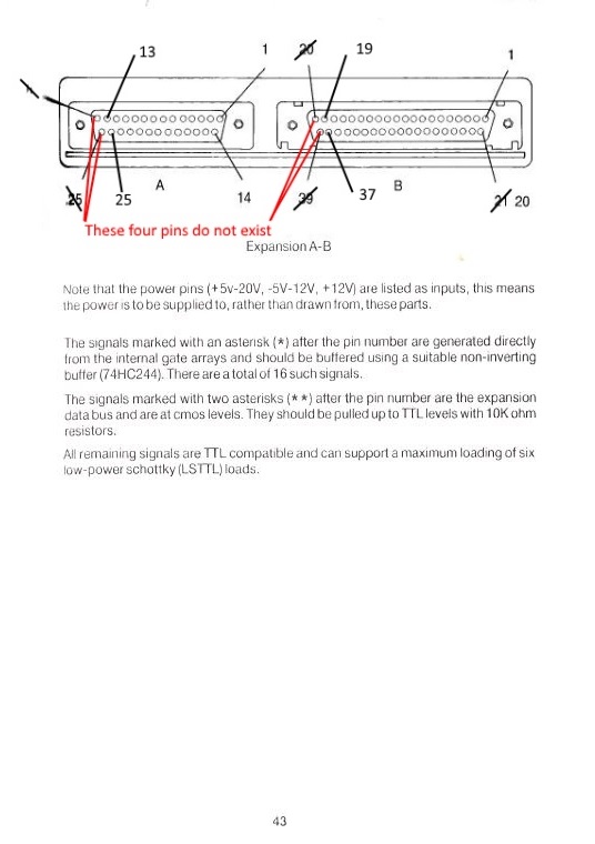